Part 1: Important Components
1) ON Semiconductor MC14584BCP Hex Schmitt Trigger
An ideal inverter is one which, when taking in as input a logic HIGH (VDD), yields a logic LOW (0V) at the output and vice-versa. Now there are inverters…and then there are Schmitt Triggers. This isn’t the name of your typical high school punk band, it’s a device invented by Otto H. Schmitt in 1934 incorporating an electrical technique called hysteresis to the normal function of the inverter. At this point it’s enough to look at this component and think “inverter” but for fits and giggles let’s look at it a little closer.
Take a look at our device’s transfer characteristic below, taken from the MC14584B datasheet. The first dataset, the one with the upward facing arrow, describes what happens when the device switches from a higher input voltage to a lower input voltage. More specifically, when a decreasing voltage at the input crosses from logic HIGH through the value VT- and towards logic LOW, the device outputs a logic HIGH. Conversely, when the opposite happens (the input voltage increases from logic LOW through the value VT+) the device outputs a logic LOW. This is similar to how an ideal inverter works except the threshold values that determine the transfer characteristic are not equal. The difference in these thresholds (VT+ – VT-) is called the Hysteresis Voltage, which can be found in the electrical characteristics section of the datasheet. For this particular device the values that matter are: VT+ = 5.3V and VT- = 4.6V.
![]()
If you didn’t get that, no worries! It’s enough to think of these devices as simple inverters for our discussion. This particular package has 6 Schmitt Trigger devices built into it. In this particular switching circuit only 2 of them are used (pins 1, 2 and pins 12, 13). It also has double-diode protection on all inputs, which is important for the possibility of ESD trying to fry our chip.
Texas Instruments has a description of the operation of a Schmitt Trigger device: Understanding Schmitt Triggers
Here’s a YouTube video of YouTube’s very own Wez Lee explaining the operation of a Schmitt Trigger in the context of a comparator-based circuit.
2) Motorola MC14016BCP Quad Analog Switch/Quad Multiplexer
This particular analog/bilateral switch is comprised of three main I/O pins: IN, OUT, and CONTROL. Take a look at the block diagram to get a better picture here.
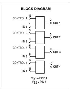
Let’s assume the IN is where your (analog) guitar signal is applied and the OUT is where you want to send your signal. When the CONTROL pin is logic LOW that signal is impeded and does not propagate through the device. However, when the CONTROL is logic HIGH your signal moves on to enjoy the adventures that await at the OUT terminal of the device.
That’s pretty much it! Oh, one important point to note is that unlike our Schmitt Trigger package this particular chip doesn’t have ESD protection on its I/Os. This is taken into account with the addition of double-diode protection in the design of our pedal’s circuit, as seen in the schematic.
Another thing that’s important to note is you don’t have to abide by the rules of INPUT or OUTPUT. With a bilateral analog switch the signal can propagate one way or the other. This will become important information when we look into the circuit’s operation.
Wikipedia has a good-enough description of analog(ue?) switches.
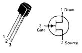
3) Motorola 2N5485 Small-Signal JFET
JFETs are commonly used in FX pedal activation controls (the classic Ibanez Tube Screamer is the first that comes to mind). In this particular circuit all you need to know is that its used as a switch. For those not familiar with the design of a JFET, take a look at the pinout below. Current can flow from the Drain to the Source terminals when a sufficient voltage is applied to the Gate terminal. If the amount of voltage is not sufficient current does not flow. Sounds like a switch, right? We’ll see how and why its used in the circuit later.
For more information on JFETs check out this ElectronicsTutorials article.
Part 2: Schematic Overview
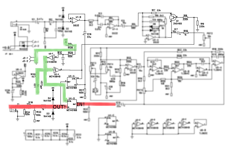
In the following schematics the green highlights logic HIGH signals and the red signifies the analog guitar signal.
Effect DISENGAGED:
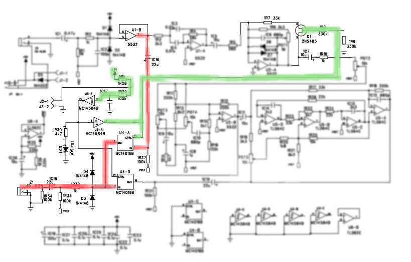
Let’s first consider the control circuit when the effect is disengaged (i.e. when the jumper terminals J2-1 and J2-2 are left open). The power source’s 9V is seen at the input (pin 13) of one of the Schmitt Trigger inverters. A logic LOW is seen at the output (pin 12) which is also connected to the LED (which is switched OFF because of insufficient current). This LOW signal is also seen at the input of the other Schmitt Trigger inverter (pin 1), driving its output (pin 2) to a logic HIGH. This logic HIGH performs two actions:
- It provides sufficient voltage to the gate of the JFET device so the clipper circuit can be bypassed. My guess is that this is to ensure that potentially amplified noise cannot be coupled or propagated to the rest of the circuit…your thoughts are valuable here!
- It sends the CONTROL input (pin 13) of the analog switch to a logic HIGH, allowing any analog signal to pass through. In this case the signal comes from the input of the pedal, is buffered by the 5532 op amp circuit, propagates through the input (pin 1) and output (pin 2) of the switch, and gets sent to the output of the pedal.
Effect ENGAGED:
Now let’s start the party by engaging our effect into action, thereby connecting J2’s terminals. In this case current from the 9V source is shunted to ground through 1R28, forcing a logic LOW at the input (pin 13) of the Schmitt Tigger. The resulting HIGH signal at the output (pin 12) turns on the LED, ceases the bypassing of the clipper circuit (by no longer supplying the JFET’s gate with sufficient voltage), and closes the other analog switch, allowing the processed signal to flow from the filter stage of the circuit to the output of the pedal.
Part 3: The Inside Look
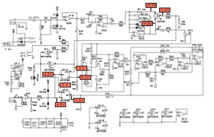
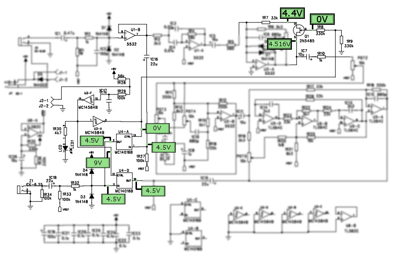
I like to be comprehensive when it comes to showing what I’ve done experimentally. The rest of this section is nothing more than a listing of what I’ve captured from the relevant zones of the pedal’s circuitry, in this case the switch control circuit.
DC Voltage Values:
The following DC values were captured when the effect was disengaged:
And here, with the pedal engaged:
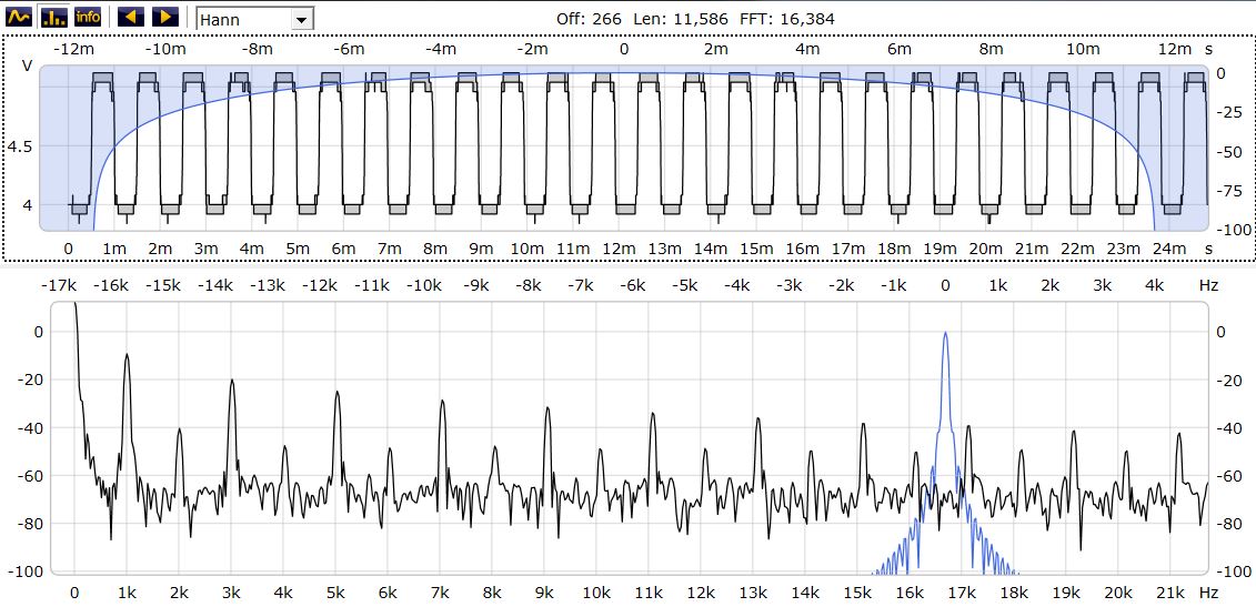
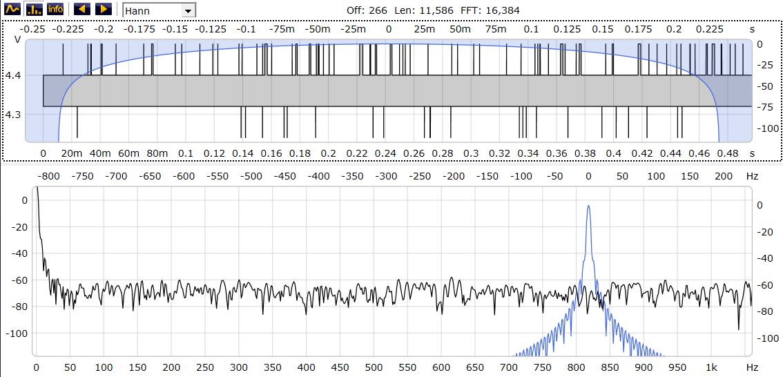
Waveforms:
The following waveforms were captured when the effect was disengaged:

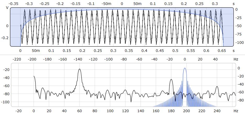
And the following, with the effect engaged:

Reference Datasheets:
MC14016BCP Quad Analog Switch/Quad Multiplexer