The last Inside Look post on Rocktron’s Rampage Distortion switching circuit sparked my interest in how other designers carry out their signal switching. After scrounging around the net I found a neat geofex article titled “The Technology of JFET Switching in BOSS and Ibanez Pedals” by R. G. Keen published in 2010. In fact, if you dig a little deeper, you can find Keen’s article (2007) published in Premier Guitar magazine which preludes this very paper. This post will document my understanding of Keen’s article.
Circuit Description & Operation

The schematic above shows the meat of the circuit design behind the bypass/effect toggle switch. This circuit is meant to send open or close signals to JFET gate terminals (not shown). The JFETs (again, not shown) are used to route the bypassed or effect signal towards the output jack of the pedal.
Think of this toggle switch like a “black-box” that has one (1) input and two (2) outputs. The input signal is obviously going to be some sort of manual switch. (This input is not shown in the schematic above, but will be introduced below.)
The two output signals of the toggle switch are taken from two separate nodes. The first is from the collector terminal of Q1 and the second from the collector terminal of Q2. One of these output signals is used to shut-off/turn on JFETs that control the signal flow of the bypass signal. The other output is used to shut-off/turn on JFETs that control the signal flow of the effect signal. It doesn’t matter which collector terminal is used for which signal path, as the toggle operation doesn’t discriminate. It only matters when you’re adding an LED signifying the pedal’s operating state. The LED is not shown in the circuit above (see below).
The BJTs in this circuit are configured to toggle between two operating modes, namely the saturation and cut-off modes. To cover the details of how these BJT modes of operation work would require a separate post, you can read about the nitty-gritty in the links provided. On a basic sense, consider the following:
- Assume the circuit is powered by 9Vdc and the base of transistor Q1 is grounded. There is now 0 volts at the base which forces Q1 to operate in cut-off mode. Thus no current flows into Q1’s collector terminal. This means 9Vdc is present at the collector terminal of Q1.
- Q1’s collector terminal is hardwired to the base of Q2 through R2, routing 9V to the base of Q2. This forces Q2 to operate in saturation mode and current rushes into the collector terminal of Q2. The voltage at Q2’s collector terminal is then pulled down to near ground.
- At this point the voltage at the collector of Q1 is about 9V while the voltage at the collector of Q2 is near 0V. This can be abstracted to say the output taken at Q1’s collector is “ON” while the output taken from Q2’s collector is “OFF”.
What happened here? We grounded the base of Q1 and the result is the collector of Q1 turned “ON” while the collector of Q2 turned “OFF”. If we disconnect the base of Q1 from ground and instead we ground the base of Q2, using similar logic, we will expect to see that Q1’s collector terminal turns “OFF” while Q2’s collector terminal turns “ON”.
From above we see that toggling the output states of this circuit can be achieved by simply alternating a ground connection between the two BJT base terminals. The trick is to design the circuitry that allows us to use a single momentary contact as our toggle footswitch. The following schematic shows the same toggle circuit with the momentary contact and LED connected to it.
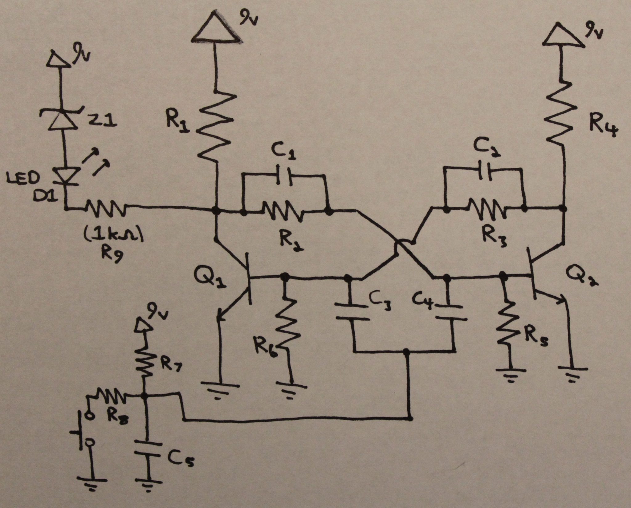
A few notes about the necessary components for this implementation:
- C1 and C2 are seen as “speed-up” capacitors used to make the toggle surer and faster. This term “speed-up capacitor” was mentioned in Keen’s paper as well as ElectroSmash’s article on the Ibanez TubeScreamer circuit.
- C3 and C4 are used to couple the base terminals and the momentary contact footswitch.
- D1 is the indicating LED signifying the output from Q1’s collector. The resistor R9 is a current limiting resistor and the zener diode Z1 is used to minimize the effect of the D1 diode current draw on the toggle circuit.
The switch circuit is made of resistors R7 and R8 as well as the capacitor C5. When the switch is not in contact charge builds on the capacitor, building up the voltage across its’ plates. When the switch is closed the cap discharges through R8 and the voltage across its’ plates decreases to 0 volts. This negative-going voltage is seen at the base terminals of the BJTs which triggers the toggle sequence to begin.
That’s it for a written explanation of the toggle circuit! Special thanks to R.G. Keen for his great work at www.geofex.com. Stay tuned for more!