Let’s talk about destructive interference. Consider two periodic signals of the same peak amplitude and frequency, say 1V peak and 440Hz, respectively. If these two signals are in phase with each other (i.e. if they are 0 degrees apart from each other) and they are added together they will constructively interfere with each other. This means the adding of the two signals will result in a doubling of peak voltage (2V instead of 1V).
If these same two periodic signals are relatively 180 degrees apart from each other and are then added together they will destructively interfere. This means the signals will cancel at all points when superimposed and the entire signal cuts out. This understanding, that you can cancel two periodic signals by shifting their relative phase 180 degrees, marks the beginning of knowing the basics of phase shifter operation.
On that, we’ll need something to provide destructive interference…a “destructive interferer”. In order to implement this “destructive interferer” we’ll need to look at a simple phase shifting unit. For this article we will only focus on one way this phase shifting unit is constructed, i.e. by using an All-Pass Filter. Why an All-Pass Filter? Well, given the explanation of interference above we’ll need to fulfill two main requirements:
- The gain of the filter must be equal to 1. This means there is no power added or taken way from the signal in the form of increasing or decreasing the overall amplitude.
- The signal at the input must be shifted in phase by 180 degrees.
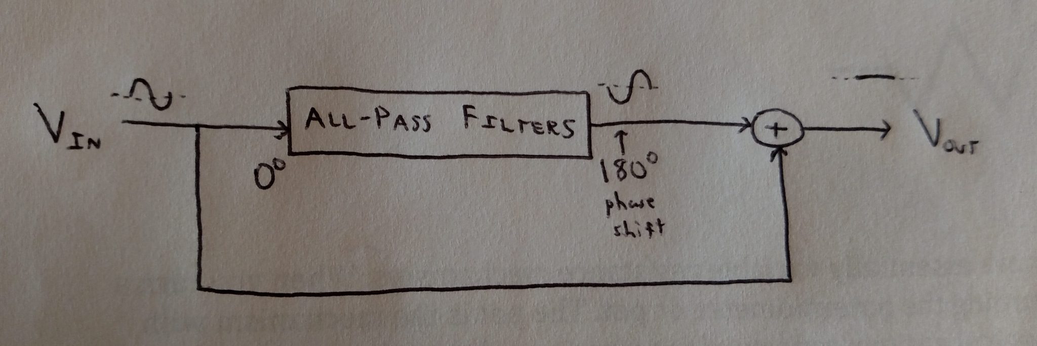
Good news: by using All-Pass Filters we can accomplish both of these requirements! From a system’s point of view we can take a look at the (not-so) pretty block diagram that is Figure 1. The input signal is fed into the All-Pass Filter block, which is tuned to a specific frequency. At the output we have that same input signal shifted in phase by 180 degrees. The output signal of the All-Pass Filter block is then added to the original input signal. At that point the two signals destructively interfere with each other, leaving behind an output signal that is seemingly zero.
Let’s look at an All-Pass Filter a little more closely. Consider the active circuit in Figure 2. This article by R.G. Keen elegantly mentions how the circuit works. This implementation takes advantage of the op amp’s ideal properties. The main property to consider here is that the current into any of the two input terminals is assumed to be zero. This allows us to disregard the op amp and analyze the branches surrounding it instead.

To analyze this circuit we need to isolate the input branch containing the RC network. The topology of how the circuit is shown may be confusing here, so consider the easier-to-follow drawing in Figure 3!

Here we have our same Vin signal applied to the circuit, but in this case it is clearer that the Vin signal oscillates about a ground reference. You see, the Vin signal can be positively or negatively valued with respect to the ground reference. This particular situation is relatively hard to analyze. Following in the footsteps of ElectroSmash’s MXR Phase 90 analysis, we’ll have to break up the circuit into two distinct cases, one when the voltage Vin is positive with respect to the reference and one when the voltage Vin is negative with respect to the reference. Why? Because from the perspective of the RC network’s output terminal the circuit looks different in both cases. In the first case (Vin > Ref) the circuit looks like a passive high-pass filter and in the second case (Vin < Ref) it looks like a passive low-pass filter. The result is the superposition of both cases. Let’s analyze!

Firstly, let’s consider Vin > Ref. We show this by grounding the terminal connected to the resistor, as shown originally in Figure 3. We have a high-pass filter, which has the following transfer function:

Second, let’s consider Vin < Ref. We show this by grounding the terminal connected to the capacitor (Figure 4) and by applying a 180 degree phase shifted signal Vin to the terminal connected to the resistor. Why? Because our frame of reference changes here. We’re looking at things “upside-down” now so we have to compensate for it by inverting our signal (phase-shifting by 180 degrees).

We have a low-pass filter, which has the following transfer function:

Both of the filters above will have the same cut-off frequency, determined by Equation 1:

Let’s assume the frequency of the input signal Vin is at this cut-off frequency. Using the notation from Figure 2, this forces the following condition:

By substitution of Omega, R1, and C1 into the two transfer functions we can calculate the phase shift of both passive filters:


Keep in mind that we initially inverted our input signal when we were first analyzing the low-pass filter configuration. This introduces a 180 degree phase shift to our calculation for the Low Pass Filter phase shift above. So now instead of a -45 degree shift we have a (-45 + 180 =) 135 degree shift. We then superimpose the two solutions onto each other:

(Here we used the polar form and complex number arithmetic to reach our result)
Voila! We have a 90 degree phase shift at the output of our RC network when it sees the cut-off frequency determined by Equation 1.

We now know that the 90 degree phase shift occurs at the non-inverting input of the op amp. What about the actual output of the All-Pass Filter? Well if we look at the branch connected to the inverting terminal (and disregard the RC network) we can safely conclude that negative feedback is being utilized. What this means is that if the op amp sees any voltage difference between its input terminals it will feed a signal back to the inverting input which works to mitigate, or correct, any voltage difference between the two input terminals.
Since the only voltage difference between the input terminals is a phase shift of 90 degrees the op amp will produce an output signal that is -90 degrees to “correct” it back to zero-phase. For our purposes the negative sign doesn’t matter, as long as a shift of 90 degrees is seen at the output we are getting what we want.
So what does all this mean? The goal of the All-Pass Filter block in a phase shifter system was to shift the signal by 180 degrees. Our active All-Pass Filter (Figure 2) only phase shifts by 90 degrees. With that in mind we can simply cascade two All-Pass Filters in series and obtain our desired 180 degree phase shift. Perfect! We then superimpose that signal to the original input signal to create the desired “destructive interference” effect.
What does this look like in the frequency domain? We obtain a notch at and around the cut-off frequency, visually showing us the destructive interference (Figure 5). In general, if we cascade n All-Pass Filters in series we will obtain n/2 notches in the frequency domain.

What’s left to do? Well a phase shifter gets its sound not only by providing destructive interference, but by shifting the frequency at which the destructive interference occurs. In effect, the notches in the frequency domain are subject to this shifting operation. Phase shifters of the type described above do this by changing the resistance of R1 by driving a resistive component with an on-board Low Frequency Oscillator (LFO) signal. There are a few ways this can be done, here are some examples:
- Photoresistors & Optoisolators (Ex. MXR Phase 100)
- Matched JFETs (Ex. BOSS PH-1 & PH-2, MXR Phase 90, DOD Phasor 201, Keeley Phase 24)
- MOSFETs
Another approach to building Phase Shifters includes the use of Operational Transconductance Amplifiers (OTAs). The shifters built around these devices are a bit more complex to go into here and deserve a post all to themselves. Some examples of OTA-based Phase Shifters include the EHX Small Stone and the Nobels Phaser PH-D.
Well, those are the (not-so-basic) basics of understanding Phase Shifter design. Contact me if you have questions or corrections. If you enjoyed this please stay tuned for more Talk Theory to Me posts! Happy Shifting!