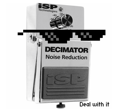
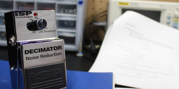
The iSP Decimator is one of the best noise reducers I’ve come across. It has virtually no tone-suck and works to cleanly remove the buzziness in your signal. It’s extremely simple to use, with only one knob for setting the noise suppression threshold.
In this post, I attempt to “stop the pop”. That’s right, a pedal that should be reducing noise is actually making noise. Particularly, an audible “pop” while switching states.
We’ll go through the circuit, it’s main components (I even drew up a tasty block diagram for you), and I’ll discuss what worked for reducing the pop.

As a member of the Reverb Partner Program and as an Amazon Associate, StompboxElectronics earns from, and is supported by, qualifying purchases.
Disclaimer: Stompbox Electronics and/or the author of this article is/are not responsible for any mishaps that occur as a result of applying this content.
The Problem with our Decimator
Introducing the iSP Decimator Noise Reduction unit! This is quite probably the best noise reducer I’ve played through thus far. There’s only one problem..it pops! You had one job Decimator!
In any case, it’s a good thing the Decimator is in our hands. What’s happening is the pedal works correctly when set to -30dB and below. Problems are only seen when disengaging the pedal with the potentiometer past the 12:00 position.
Engaging the pedal is fine but once we decide to disengage, it lets out a noticeable “pop” in the output. Turning the potentiometer clockwise from 12:00 makes the popping sound even more noticeable.
So we see two things here: (1) The popping intensity is dependent on the position of the potentiometer and (2) the popping only occurs when disengaging the pedal. Keep these in mind as we continue.
Where could pedal pop come from?
So now we have some clues. As an aside, when pedal-popping complaints arise it is usually a result of a DC current snaking its way into the signal path and eventually into the pedal’s output signal.
Now I will admit to not knowing all the ways this can happen, but the primary cause is a build up of charge. This charge build-up only results in pedal pop when it can quickly make its way into the output signal. The quicker the discharge, the “shriller” the pop. The slower the discharge, the “duller” the pop.
The same can be said on how filtered the popping noise is. If a pop is low-pass filtered, it can be transformed into a “thud”-like sound. You can read more about that here.
As an Amazon Associate, Stompbox Electronics is supported by and earns from qualifying purchases:

Diving Into the iSP Decimator Circuit
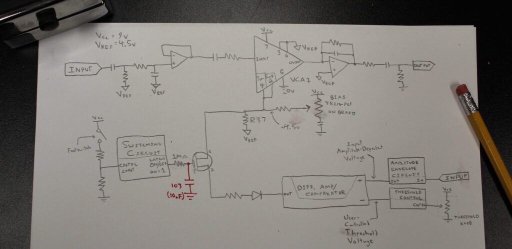
After some careful thought the next thing to do is take a look at the schematic and try to pin-point possible areas where charge build-up can occur. But first…we need a schematic. I was pointed to Fred Brigg’s La Revolution Deux blog and found a schematic for an iSP Decimator model similar to what I had. It’s not perfect, but that’s what I had to work with.
It’s also nice to have the datasheets handy for any ICs or transistors onboard. This Decimator only uses 3 types of ICs:
- THAT2181C – Voltage Controlled Amplifier (VCA)
- LF353 – Dual JFET Op Amps
- HEF4013 – Dual D-Type Flip-Flop
And 3 transistors:
Reading through some of the datasheets I suspect the VCA chip is intercepting a DC input voltage. Though, this is ruled out since there happens to be an input coupling capacitor which should thwart any chance of a DC voltage popping up at the input of the VCA.
Eventually I took another look at the schematic and realize the switching circuitry for the model I have isn’t conveyed. This is directly related to the original problem, so maybe the solution lies in that area of the board…
I pulled flexed my reverse engineering muscles and traced out the Decimator’s switching circuit (mock schematic below)
Tracing out the circuit revealed a 2N5484 JFET transistor used to switch the pedal on and off. It’s important to understand conceptually how this switching circuit interacts with the rest of the circuit, so I’ll explain the inner workings of how this pedal switches ON and OFF.
The iSP Decimator Switching Circuit
What happens when the iSP Decimator is OFF?
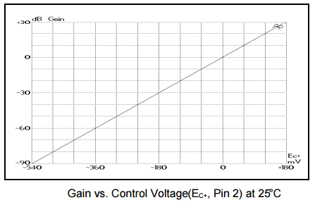
When the pedal is disengaged, the gate voltage of the JFET is too low to allow current through the source and drain terminals. This severs the movement of the input signal from the VCA’s operation, leaving only a virtual ground applied to Ec+ (pin 2) of the VCA (4.5V, set by an on-board trimpot). This DC voltage is constant and, at 4.5V, the chip sees a virtual ground. This is because pin 6 of the VCA is also seeing 4.5V, so in the chip’s perspective the Ec+ pin is at a constant reference voltage.
Looking at the chart below, when the chip sees a control voltage of 0V (in relation to pin 6) the VCA gain is set to 0dB. This means the chip doesn’t amplify or attenuate. Whatever signal you put into it should also be received at the output.
What happens when the iSP Decimator is ON?
Now let’s understand what’s going on when the pedal is engaged. Take yet another look at the chart above. If we decrease our control voltage the amount of gain we apply to the input signal proportionally decreases. Essentially, when engaged, the circuit allows a voltage variation at the Ec+ control pin. This controls the amount of gain/attentuation the VCA applies to the input signal.
How does the iSP Decimator attenuate?
The iSP Decimator is using Ec+ control voltage pin to achieve attenuation. The Ec+ control voltage is a function of two things:
- The amplitude envelope of the input signal , and
- A user-controlled threshold voltage set by the potentiometer.
If the input signal’s amplitude envelope is below the threshold voltage, then the circuit decreases the Ec+ control voltage accordingly. The VCA attenuates the signal.
If the input signal’s amplitude envelope is above the threshold voltage, then the circuit increases the Ec+ control voltage such that the VCA eases off with the attenuation.
So how does the circuit increase or decrease the control voltage? Answer: current!
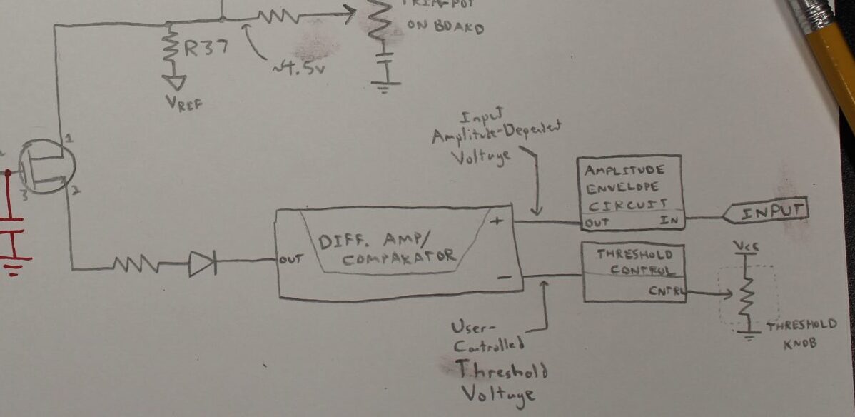
Firstly, both the input signal amplitude envelope and the threshold voltage are sent to a differential amplifier (which we can think of as a comparator for ease of discussion). This component increases or decreases it’s output voltage based on the comparison of its two input signals. This voltage is seen at the cathode side of a diode. The anode side sees the drain terminal of the 2N5484 FET.
If the voltage across the diode is positive enough, current starts to sink through the FET and resistor R37. This current produces a voltage difference across R37 that pulls the control voltage lower than virtual ground. This in turn provides the attenuation and, hence, “noise” reduction based on the plot from before.
How does this help us?
Now for the main take-away: When the pedal goes from being engaged to being disengaged (i.e. when the gate voltage of the FET is suddenly hit with 9V from the switching circuit) the current providing the drop in control voltage ceases and the control voltage increases (or decreases) back to it’s original virtual ground of 4.5V.
This self-correction of control voltage is sudden. So sudden that this popping sound could be originated by it’s occurrence. If a fast voltage transition is the suspect, let’s find a way to slow down this voltage transition.
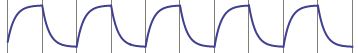
Let’s think about what causes this voltage transition on the control pin. In our case, it’s the sudden change generated by the switching circuit applied to the FET gate terminal. This type of step-change signal is depicted below.
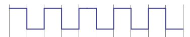
All we need to do is smooth out this transition (image below) while making it last long enough to not hear a “pop” in the output. We can achieve this by constructing an RC circuit at the gate terminal, being careful to choose component values that allow a slower voltage transition.
Repairing the iSP Decimator
The circuit already utilizes a 1M-ohm resistor at the gate terminal. What needs to be added is a capacitor between the gate terminal and ground (0V). I tested the pedal’s operation with a 103 ceramic capacitor branched between the gate terminal and ground. This allowed a softer fade out of the current through the FET which ultimately eliminated the “pop.”
Awesome! All that just to add a little capacitor. We got very technical this time, but I hope you learned something along the way.
Meet the Author:

Hi, I’m Dominic. By day, I’m an engineer. By night, I repair and modify guitar effects! Since 2017, I’ve been independently modifying and repairing guitar effects and audio equipment under Mimmotronics Effects in Western New York. After coming out with a series of guitar effects development boards, I decided the next step is to support that community through content on what I’ve learned through the years. Writing about electronics gives me great joy, particularly because I love seeing what others do with the knowledge they gain about guitar effects and audio circuits. Feel free to reach out using the contact form!
Spotlight
This fix was done for Cody Morse. Cody operates Afterglow Studios in Tonawanda, NY & is soothing souls in the Buffalo, NY-based band, Deadwolf.
The Tools I Use
As a member of Amazon Associates, Stompbox Electronics earns and is supported by qualifying purchases.