So I’ve been working on a BOSS CH-1 mod and in doing so I’ve been increasingly interested in how Low Frequency Oscillator (LFO) circuits are designed and constructed. Its worth investing time on the topic, especially since when diving into modulation effects you quickly find out that LFOs exist at every corner. Most LFOs are very simply constructed with Rate and Depth parameters, but one relatively popular DIY pedal project caught my attention – the Tremulus Lune. This DIY tremolo project was originally developed by Dan Green from 4ms Pedals and is available in kits or pre-built from their website.
The reason why the Lune was so interesting to me was the number of parameters it boasts. Not only that, but putting even more research into the circuit revealed the variety of mods that are able to be designed around it. In the coming paragraphs I try to both introduce the type of oscillator used in the Lune as well as a conceptual view into how the LFO circuit works.
Note: In order to understand the following topics you’ll need to know some basics of current flow and voltage distribution in basic op amp and RC circuits. Look at the Mimmotronics Resources page for some online information on these topics.
Relaxation Oscillators
The type of oscillator used in the Tremulus Lune is called a relaxation oscillator. Relaxation oscillators usually produce non-sinusoidal periodic waves, like a triangle wave or a square wave. Wikipedia says it best:
Relaxation oscillations are characterized by two alternating processes on different time scales: a long relaxation period during which the system approaches an equilibrium point, alternating with a short impulsive period in which the equilibrium point shifts.
By that definition we can deduce the following:
- The system needs to have 2 equilibrium points to oscillate between. The Lune accomplishes this by employing a hysteretic comparator.
- There must be some way to define the relaxation time, which is the time it takes for the system to “relax” to one of the 2 equilibrium points. An RC network is employed for this task.
Note that there are other ways to build relaxation oscillators. For example, the analog version of the BOSS CH-1 utilizes a dual op amp configuration. I’ll cover dual op amp LFOs and other types of oscillators in future posts. For now, lets focus on the Lune!
The Tremulus Lune LFO
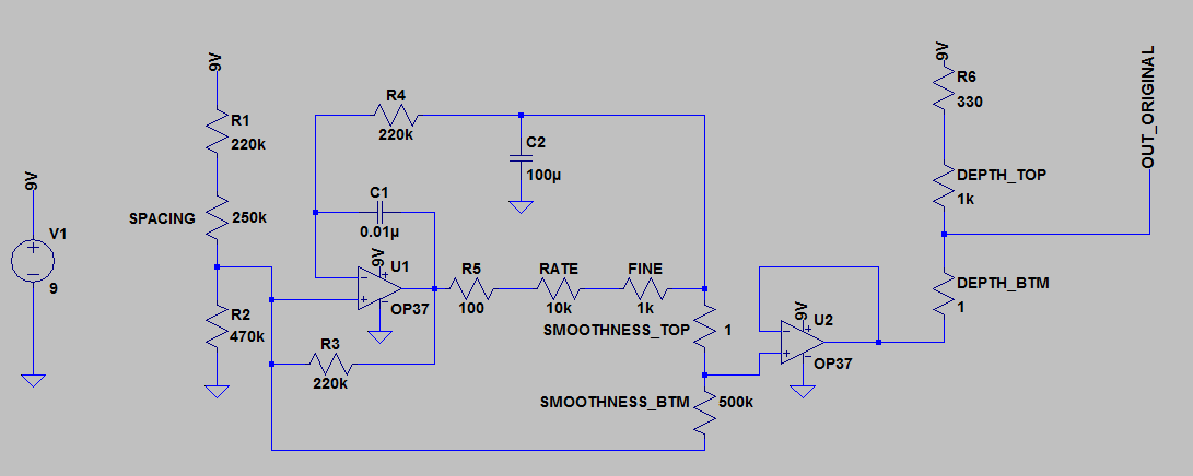
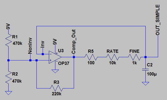
The Tremulus Lune’s LFO is modeled in Figure 1 using LTSpice. The basic parameters are: Rate, Depth, Fine, Smoothness, and Spacing.
To simplify the discussion, let’s strip this circuit down to the basics. Figure 2 shows an extremely simplified version of the Tremulus Lune and Figure 3 shows the important signals we’re going to be talking about.
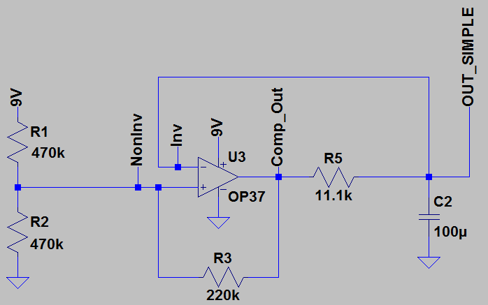
The op amp sees a slight input offset voltage when the circuit is provided power. This input offset voltage is amplified by the gain of the op amp and eventually the oscillations start due to positive feedback.
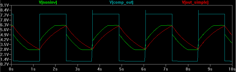
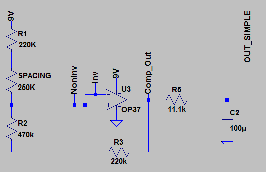
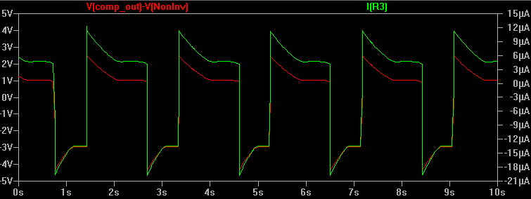
When our circuit is oscillating the comparator outputs a square wave. The cyan-colored signal is the output of the op-amp comparator. A square wave essentially alternates between two values. In the simulation, our square wave alternates between 7.86V (HIGH value) and 1.14V (LOW value). The amount of time the square wave is HIGH relative to its total period is called the duty cycle and is displayed as a percentage. For example, a square wave with a 50% duty cycle is HIGH half of its period. A 75% duty cycle suggests the wave is HIGH for 3/4ths of its period, and so on.
The green signal represents the voltage at the non-inverting terminal of the op amp. We can see that for each HIGH and LOW value of the comparator output there’s a corresponding HIGH and LOW value that the non-inverting terminal voltage eventually settles towards until the next step-change occurs. The corresponding HIGH and LOW values on the non-inverting terminal are 6.235V and 2.764V, respectively.
The red signal is the output of the RC network, which also happens to be the output of the LFO. In the simplified version this signal is directly fed back to the inverting terminal of the op amp. Understanding the interactions between these signals and components is best described in steps:
- When the comparator output is HIGH the capacitor C2 starts charging and thus its voltage increases at an exponential rate. This voltage is also seen at the inverting terminal.
- When the inverting terminal voltage starts to cross above the non-inverting terminal voltage the comparator switches its output state to a LOW value. Due to positive feedback, the non-inverting terminal voltage also switches to its LOW value, which is determined by hysteresis.
- The capacitor C2 sees, through resistor R5, a LOW value at the comparator output which is now lower than the voltage across the capacitor. Because of this voltage difference, current starts to sink into the op amp’s output and the cap starts to discharge. Again, this capacitor voltage is seen at the inverting terminal.
- Once the inverting terminal voltage crosses slightly below the non-inverting terminal voltage the comparator switches its output state from LOW to HIGH, and the sequence starts over.
The Spacing Parameter
In the description above the non-inverting terminal voltage is used as a reference. Not only that, but its reference voltage alternates between two values and is done using a technique called hysteresis. By way of hysteresis it’s apparent that resistors R1, R2, and R3 determine the HIGH and LOW voltage levels on the non-inverting terminal signal. If we’re able to alter one of those 3 resistances the hysteresis voltage levels can be varied.
So…what’s this Spacing parameter do? Let’s look at the simplified schematic, but with the Spacing parameter added. (Figure 4) You will see that R1 from the previous simplified schematic now has another resistance “SPACING” on the same branch, which we will alter below.
And let’s also take a look at some plots. Figure 5 shows the non-inverting terminal voltage, comparator output voltage, and LFO output voltage when the SPACING pot is set to 0Ω. Figure 6 shows the same signals when SPACING is at 250kΩ and Figure 7 shows them at 500kΩ.
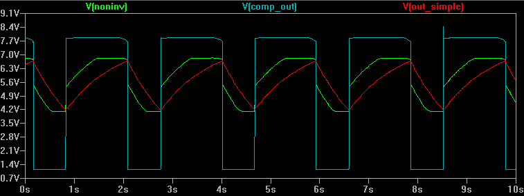
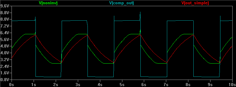
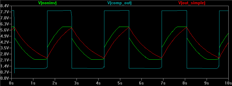
The most obvious property that changes is the Duty Cycle of the comparator’s output signal. How does this happen? The RC network needs both charging and discharging current paths. When the capacitor is charging it sinks current primarily from the output of the op amp, but some current is supplied through the hysteresis resistor R3. The amount of current supplied through R3 is determined by the voltage difference across R3. The Spacing resistor controls this voltage difference via setting the voltage references on the NonInv node.
When we set the Spacing resistance to a lower value we effectively increase the reference voltage at the non-inverting terminal-side of R3. As a result, when the comparator output-side of R3 is LOW there is a larger absolute voltage difference across R3 compared to when the output is HIGH (see Figure 8). The larger voltage difference suggests more current is sourced through R3 and the capacitor charges that much quicker. On the flipside, when the output is HIGH the amount of current sinking through R3 is proportionally decreased. In this way the Spacing resistor can be used to change the duty cycle without majorly changing the output frequency of the LFO.
The Rate & Fine Parameters
To understand how the Rate and Fine Parameters work you’ll need some background on RC circuits. Check out this page for a quick overview. After that, take a look at the simplified schematic with the Rate and Fine pots added in (Figure 9).
The main function of the Rate and Fine pots is to adjust the frequency of the LFO. The frequency of the LFO is dependent on the rate by which C2 charges and discharges via the RC network resistance (made up of R5, RATE, and FINE). By simulation you should expect a frequency range of 416mHz to 40.5Hz. If the goal is to modify the Lune’s frequency range, then the RC network’s resistance is where your interest should be.
The Smoothness Parameter
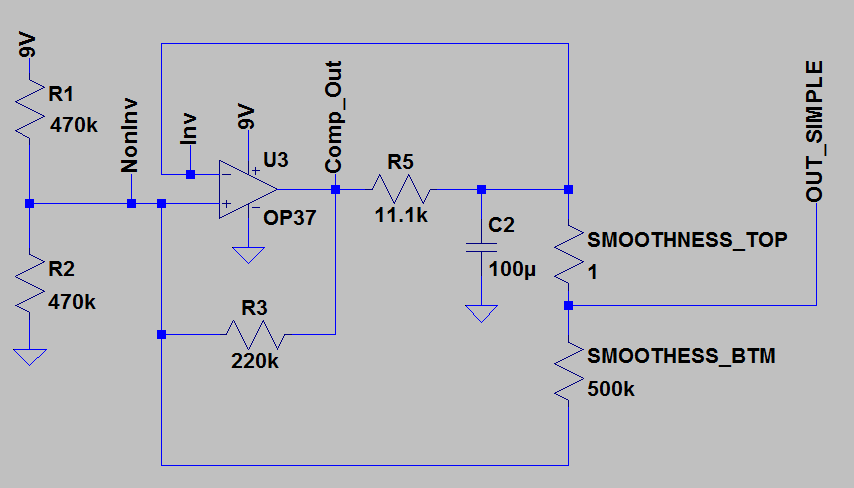
The Smoothness pot acts as a cross-fader control between the RC network output and the voltage signal at the NonInv node. The NonInv node boasts some high-frequency transient properties. Therefore, when crossfaded with the LFO output signal, the output becomes more jagged and less smooth. Figure 10 shows the simplified schematic with the Smoothness parameter added as two resistors.
The Depth Parameter
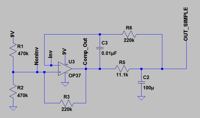
The main oscillating section of the circuit (the RC network & hysteretic comparator) acts in a closed system with voltage and current levels that need to be maintained. The node that we’ve been using to plot the LFO output is not suitable for driving an LED since that requires a relatively large current draw that could “weigh down” the oscillator (see Loading Effect). As a result we need to employ a voltage follower which is going to be able to supply the necessary amount of current to an LED driver circuit without loading the oscillator system too much. This can be seen in Figure 11 along with the Depth potentiometer.
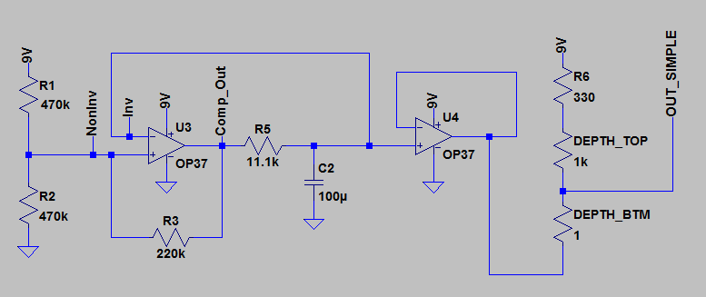
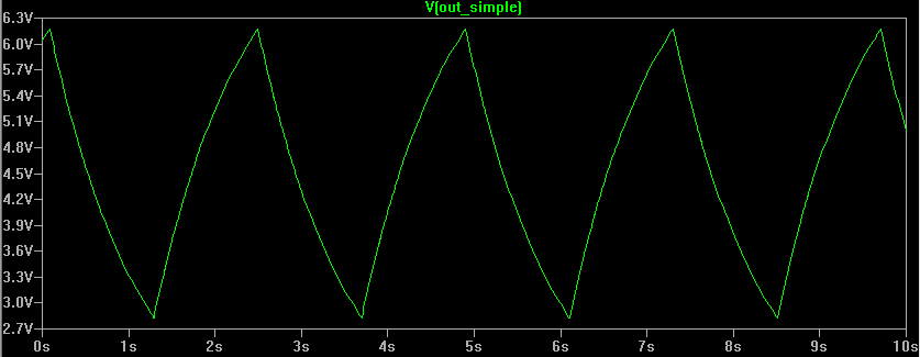
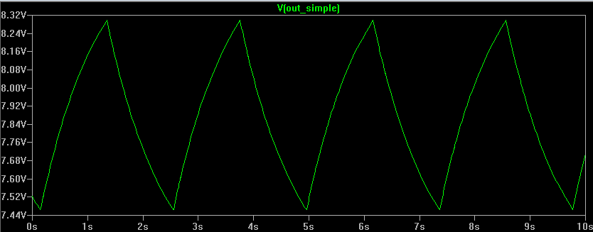
The OUT_SIMPLE node is used to apply the LFO voltage to an LED which, in the Lune, will be used to vary a photoresistor in the pedal’s signal path. The Depth parameter acts as a Level pot for the LFO. Figure 12 shows the output with the values in Figure 11. Figure 13 shows the output with DEPTH_TOP = 1 and DEPTH_BTM = 1k.
Other Features
Let’s take a look at the comparator output signal in Figure 3. There we see that there are voltage spikes occurring at the edges of the square wave. To mitigate these spikes and to prevent them from propagating to the LFO output we need to introduce C3 and R6, shown in Figure 14.
Capacitors generally let AC signals “pass through” them, but “blocks” DC signals from passing through. The voltage spikes are, by their nature, high-frequency transient AC signals. When they occur at the Comp_Out node they make their way through C3 and into the Inv node (instead of through R5, because of the “apparent” electrical short created by C3.) At this point these signals see the resistance of R6, which forms an additional low-pass filter with C2. The cut-off frequency of the low-pass filter formed by R6 and C2 is so small that the voltage spikes are almost entirely attenuated at the output. If these components were left out the player would hear a “popping” sound in sync with the frequency of the LFO.